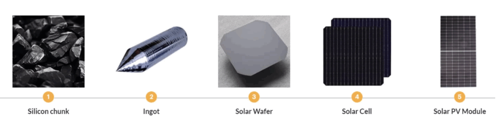
Popup Logo

Technology

Built on Precision, Powered by Automation

Advanced Manufacturing Features

Our solar manufacturing unit uses fully automated lines to ensure precision, quality, and high output. With a capacity of XXX, our facilities support both domestic and export demand.

Multi-busbar & Half-Cut Cell
Advanced Lamination & Framing
Eco-Responsible Processes

SOLAR PV TECHNOLOGY

Crystalline silicon (c-Si) solar technology dominates the global photovoltaic (PV) market, accounting for over 90% of installations due to its proven efficiency, durability, and scalability. Below is an overview of key c-Si technologies:

1. Monocrystalline Silicon (Mono-Si)

  • Structure: Single crystal lattice (Czochralski process)
  • Efficiency: 22–24% (up to 26.7% lab)
  • Advantages: High space efficiency
  • Considerations: Higher cost

2. Polycrystalline Silicon (Poly-Si)

  • Structure: Fragmented crystal structure
  • Efficiency: Around 15–17%
  • Advantages: Lower production cost
  • Considerations: Less efficient, more space

3. PERC (Passivated Emitter and Rear Cell)

  • Structure: Rear passivation layer
  • Efficiency: Up to 23.5%
  • Advantages: Better low-light performance
  • Considerations: May suffer from LID/PID

4. TOPCon (Tunnel Oxide Passivated Contact)

  • Structure: Tunnel oxide + doped polysilicon
  • Efficiency: ~23% (25% lab)
  • Advantages: High efficiency, better thermal performance
  • Considerations: More complex & costly

5. Heterojunction Technology (HJT)

  • Structure: Crystalline + amorphous silicon
  • Efficiency: ~24% (up to 26.7% lab)
  • Advantages: Excellent in high heat, high bifaciality
  • Considerations: Costly & production sensitive

6. Interdigitated Back Contact (IBC)

  • Structure: All contacts on rear; no front-side shading
  • Efficiency: Up to 24.7%
  • Advantages: High light absorption, sleek appearance
  • Considerations: Complex and costly to manufacture

7. Perovskite Solar Cells

  • Structure: Perovskite compounds as light absorber
  • Efficiency: Lab over 29% (tandem)
  • Advantages: Low-cost, high potential efficiency
  • Considerations: Stability and scale-up still evolving

8. Tandem Solar Cells

  • Structure: Multiple PV layers for wide-spectrum absorption
  • Efficiency: >30% in lab (perovskite-silicon)
  • Advantages: Exceptional potential efficiency
  • Considerations: Complex and less stable at scale

SOLAR PV TECHNOLOGY

Crystalline silicon (c-Si) solar technology dominates the global photovoltaic (PV) market, accounting for over 90% of installations due to its proven efficiency, durability, and scalability. Below is an overview of key c-Si technologies:

Monocrystalline Silicon

1. Monocrystalline Silicon (Mono-Si)

  • Structure: Single, continuous crystal lattice.
  • Efficiency: Up to 26.7% lab efficiency; 22–24% commercial.
  • Advantages: High space efficiency.
  • Considerations: Higher cost due to complex manufacturing.
Polycrystalline Silicon

2. Polycrystalline Silicon (Poly-Si)

  • Structure: Multiple silicon crystals melted together.
  • Efficiency: 15–17%.
  • Advantages: Lower production cost.
  • Considerations: Lower efficiency; requires more space.
PERC Technology

3. Passivated Emitter and Rear Cell (PERC)

  • Structure: Passivation layer on rear side reflects light.
  • Efficiency: Up to 23.5% commercial.
  • Advantages: Better low-light performance.
  • Considerations: Susceptible to LID and PID.
TOPCon

4. Tunnel Oxide Passivated Contact (TOPCon)

  • Structure: Tunnel oxide + doped polysilicon for better electron passivation.
  • Efficiency: Lab >25%, commercial ~23%.
  • Advantages: Higher efficiency & better temperature coefficient.
  • Considerations: Complex manufacturing & higher cost.

Each of these technologies offers unique benefits and is suited to different applications and budgets. The choice depends on installation space, budget, and specific energy needs.

Get the Details You Need

XXX MW capacity. Supporting India & Export Markets.
Cart (0 items)